
About Allwin21
Founded in 2000 and located in Silicon Valley, California, Allwin21 is an engineering-driven semiconductor equipment company serving advanced semiconductor customers worldwide.
Our core equipment areas include Rapid Thermal Processing / RTP systems, plasma asher / descum equipment, plasma etch / RIE systems, sputter deposition equipment, metal film metrology equipment, and semiconductor equipment upgrade solutions.
Allwin21 supports compound semiconductor, silicon, photonics, optoelectronics, MEMS, power devices, RF devices, automotive electronics, optical communication, aerospace, university research, and advanced process development customers.
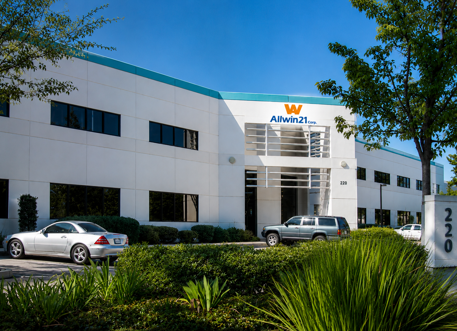
Allwin21 Headquarters & Engineering-Driven Foundation
The Foundation of Our Engineering-Driven Philosophy
Before founding Allwin21 in 2000, our founder spent more than 15 years in the semiconductor industry after graduating with a major in Semiconductor Devices. His work covered Metrology Engineering, Process Engineering, Equipment Engineering, direct responsibility for operating a compound semiconductor fab, and leadership in building semiconductor fab lines from the ground up.
Those years revealed a reality that still exists today: compound semiconductor fabs often use equipment platforms originally developed for the silicon industry, but their operational requirements are different. Process stability, equipment uptime, troubleshooting efficiency, maintainability, spare parts continuity, qualified process results, and production yield are all part of the real equipment requirement.
This understanding became the foundation of Allwin21’s Engineering-Driven philosophy. For more than 25 years, Allwin21 has applied this thinking to equipment design, modernization, upgrade solutions, software development, and customer support. It also shaped our Process-Oriented Software approach: equipment control, diagnostics, process data, and engineering information built around the daily work of process engineers, equipment engineers, and manufacturing teams.
Our Engineering DNA
Born from Semiconductor Fab Experience
Process and Equipment Thinking Together
From Upgrade Experience to Modern Rebuild Equipment
Early Upgrade and Modernization Experience
Focused Rebuild Equipment and Upgrade Service
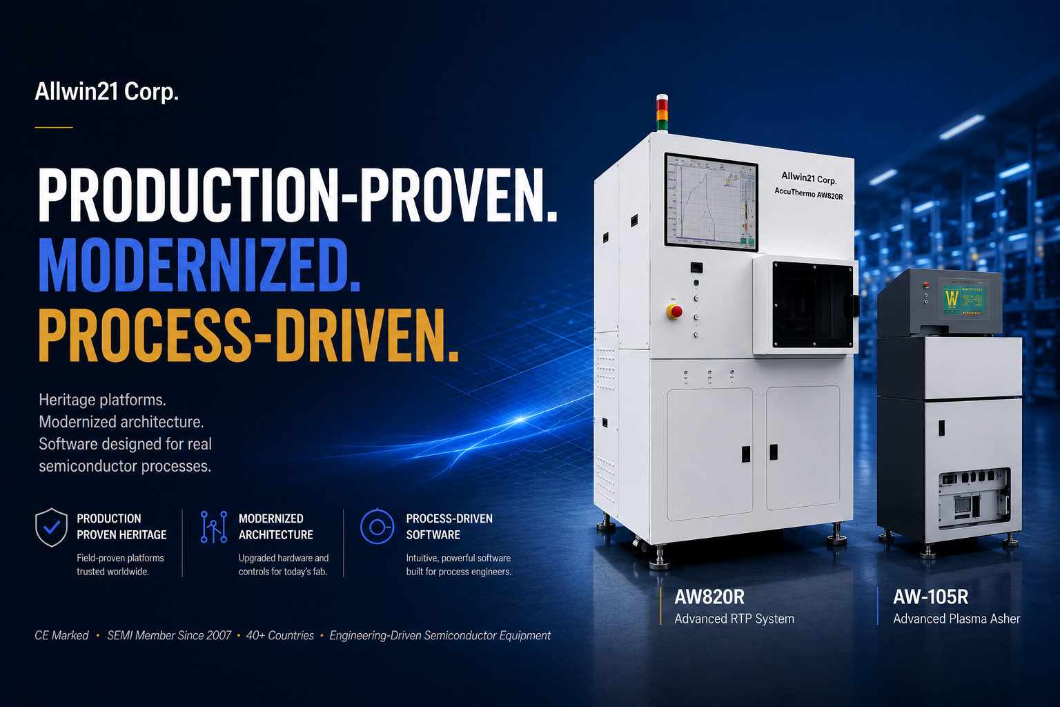
What Makes Allwin21 Equipment Different
Production-Proven Platform First
Modernized Hardware Architecture
Software Written for Real Engineers
Lower Adoption Risk for Customers
Engineering-Driven Sales and Service Philosophy
The Right Proposal Matters
Service Based on Engineering Diagnosis
Compound Semiconductor Fab Equipment Realities
Different Fab Requirements
8-inch and 12-inch silicon fabs are usually built around high-volume, standardized production, mature OEM support, and highly automated fab operation. Compound semiconductor fabs often run process-qualified tools in mixed toolsets for RF, photonics, power devices, LED, GaN, SiC, InP, GaAs, and specialty applications.
Why Legacy Tool Support Is Difficult
Large OEM support models are often built for large installed bases and standardized silicon production. Many compound semiconductor fabs still depend on legacy tools with no full OEM support, obsolete controllers, PCB failures, used spare markets, and independent service sources.
Semiconductor Dry Vacuum Pump: Atlas Copco (Edwards Vacuum) Ebara Corporation Pfeiffer Vacuum GmbH Kashiyama Industries Beijing Grand Hitek SKY Technology Development Ningbo Baosi Energy Equipment LOTVACUUM Taiko Kikai Industries Busch Vacuum EVP Vacuum Technology Scroll Laboratories Inc ULVAC Inc Highvac Corporation Osaka Vacuum Ltd; Capacitance Diaphragm Gauges: Inficon MKS Agilent Setra Pferffer Canon Anelva Leybold GmbH ULVAC Nor-Cal Brooks Kurt J. Lesker Thyracont InstruTech Azbil Horiba Atovac;Semiconductor Back-End Test Equipment : Accretech TEL Semics Fittech Sidea Semiconductor FormFactor Advantest Teradyne Cohu Hangzhou Changchuan Technology YC Corp Beijing Huafeng Test & Control Technology Hon Precision SPEA Shibasoku Macrotest PowerTECH HON PRECISION, INC JHT Design Co.,Ltd Boston Semi Equipment SESSCO Technologies SYNAX Microtec Handling Systems GmbH Tesec Inc Techwing Kanematsu UENO SEIKI NAGANO Shanghai Cascol Shenzhen Semishare MPI Corporation Micronics Japan ASM Pacific Technology Everbeing MarTek Micromanipulator Signatone Corporation HiSOL, Inc KeyFactor Systems Wentworth Laboratories APOLLOWAVE MicroXact KeithLink Technology Ecopia Shenzhen Cindbest Technology ESDEMC Technology Lake Shore Cryotronics Wuhan Jingce Electronic Technology Exatron;KrF and ArF Photoresist: TOKYO OHKA KOGYO CO.LTD. (TOK) JSR Shin-Etsu Chemical DuPont Fujifilm Sumitomo Chemical Dongjin Semichem YCCHEM Co.Ltd Xuzhou B & C Chemical Red Avenue Crystal Clear Electronic Material SK Materials Performance (SKMP) Xiamen Hengkun New Material Technology Zhuhai Cornerstone Technologies SINEVA Guoke Tianji Jiangsu Nata Opto-electronic Material Shanghai Sinyang Semiconductor Materials Merck KGaA (AZ); Optical Film Thickness Monitor : Optorun Guangdong Huicheng Vacuum Technology Zhongke Weishi Technology Wuhan eoptics Technology OELABS Chengdu Guotai Vacuum Equipment KLA HORIBA Scientific LayTec AG Eddy Co. Angstrom Advanced Inc. Sentech Instruments GmbH Nanovea INFICON Intellemetrics Global Ltd Otsuka Electronics AccuStrata Inc. Colnatec LLC;Optorun Guangdong Huicheng Vacuum Technology Zhongke Weishi Technology Wuhan eoptics Technology OELABS Chengdu Guotai Vacuum Equipment KLA HORIBA Scientific LayTec AG Eddy Co. Angstrom Advanced Inc. Sentech Instruments GmbH Nanovea INFICON Intellemetrics Global Ltd Otsuka Electronics AccuStrata Inc. Colnatec LLC;disc polishing machine: Ri-Thai Perlon NTEC Monosuisse Tai Hing Ruichang Special Monofilament Jintong Jarden Applied Materials VitasheetGroup Toray Superfil Products Teijin Judin Industrial Marmik;EUV Mask Blanks: AGC Inc Hoya S&S Tech Applied Materials Photronics Inc; Cryocoolers: Sumitomo Heavy Industries Thales cryogenics AIM Brooks Automation Inc Cryomech Inc Ricor – Cryogenic & Vacuum Systems Cobham DH Industries Sunpower Inc RIX Industries Lihan Cryogenics Advanced Research Systems; Nanoindentation Tester: Anton Paar Bruker KLA Helmut Fischer Optics11 Life ZwickRoell Semilab Micro Materials Elionix FemtoTools NANOVEA; CVD Susceptor : SGL Carbon Schunk Xycarb Technology TOYO TANSO Tokai Carbon Momentive Technologies CoorsTek ZhiCheng Semiconductor Bay Carbon Mersen Ningbo Hiper LIUFANG TECH Hunan Xingsheng Chengdu Ultra Pure Applied Materials; Semiconductor Rapid Thermal Process Oven (RTP) : Annealsys NPOS Technologies UniTemp GmbH Unitemp Germany Allwin21 AMETEK Process Instruments Plasma-Therm JTEKT Thermo Systems PhotonExport Anargya Innovations & Technology SemiStar Corp Modular Process Technology Corp Surface Science Integration XERION BERLIN LABORATORIES centrotherm ADVANCE RIKO LEGUAN LarcomSE Giant Tek Corporation Beijing E-Town Semiconductor Technology Shenzhen Kejing Star Technology Company; 2-Inch Fully Automatic Three-Temperature Test Probe Station : Semics FormFactor Tokyo Seimitsu Tokyo Electron Semishare Electronic MarTek (Electroglas) Wentworth Laboratories ESDEMC Technology MPI Shen Zhen Sidea FitTech Hangzhou Changchuan Technology; 3D Scanner: Shining 3D Align Technologies Medit Planmeca Oy 3Shape Straumann (Dental Wings) Keyence Dentsply Sirona Envista(Carestream) FARO Scantech Midmark(3M) ZEISS Nikon Metrology Creaform Artec3D Up3D ZG Technology Thor3D Peel3D Freqty Fussen Technology Runyes Mantis Vision I2S Gt-Medical Rangevision SMARTTECH3D Met Optix Polyga; Semiconductor Etch Equipment: Lam Research Allwin21 SemiStar TEL Applied Materials Hitachi High-Tech Oxford Instruments SPTS Technologies Plasma-Therm GigaLane SAMCO AMEC NAURA; Laser Annealer: Mitsui Group (JSW) Sumitomo Heavy Industries SCREEN Semiconductor Solutions Veeco Applied Materials Hitachi YAC BEAM EO Technics Beijing U-PRECISION Tech Shanghai Micro Electronics Equipment Chengdu Laipu Technology Hans DSI; Molecular Drag Pumps: Pfeiffer Edwards Vacuum Leybold Agilent Technologies ULVAC Ebara Technologies Osaka Vacuum Shimadzu Busch Vacuum Becker Pumps Yuanhua Industrial Duniway Stockroom; PVD Thin Film Consumable : Materion Umicore Heraeus Kurt J. Lesker Plansee Angstrom Sciences SCI Engineered Materials Stanford Advanced Materials EVOCHEM Alcadyne Tosoh SMD; PVD (Physical Vapor Deposition) Coaters : Von Ardenne Evatec Veeco Instruments Hanil Vacuum BOBST Satisloh IHI Hongda Vacuum Platit Lung Pine Vacuum Beijing Power Tech SKY Technology Impact Coatings HCVAC Denton Vacuum ZHEN HUA Mustang Vacuum Systems KYZK; Vacuum Evaporation Material: NICHIA Materion Umicore Stanford Advanced Materials Angstrom Engineering Kurt J. Lesker Company ZhongNuo Advanced Material Beijing Goodwill Metal Technology Changsha Xinkang Advanced Materials GRIKIN Advanced Material Co., Ltd. Vital Materials Co., Ltd. American Elements Furuya Metal Co., Ltd. LTS Research Laboratories EVOCHEM Advanced Materials; Magnetron Sputtering Sources: Applied Materials Chemours Tokyo Electron Corning Alfa Laval Hitachi High-Tech ThyssenKrupp Metso Faurecia Kohler MeiVac PVD Products AJA Internationa Kurt J. Lesker Company Plasmionic Technologies Gencoa Materials Science Scienta Omicron RBD Instruments; PVD (Physical Vapor Deposition) Coaters : Von Ardenne Evatec Veeco Instruments Hanil Vacuum BOBST Satisloh IHI Hongda Vacuum Platit Lung Pine Vacuum Beijing Power Tech SKY Technology Impact Coatings HCVAC Denton Vacuum ZHEN HUA Mustang Vacuum Systems KYZK; Quartz Tube products: Technical Glass Products Robuster Quartz San Jose Delta Associates Allen Scientific Glass A.M. Quartz Corporation Desert Glass Works Donghai County Alfa Quartz Products G. Finkenbeiner Giantek Quartz G.M. Associates GWI Sapphire Heraeus Quartz America Jelight Company Jiangsu Pacific Quartz JNS Glass & Coatings Macrobizes Medivision Morgan Advanced Materials National Scientific Company Nippon Electric Glass Pacific Quartz Quality Quartz Of America Quick Gem Optoelectronic S&T Sentro Tech Corporation Shenzhen Solarvalley Technology Development SICO Technology GmbH Suzhou Quartz Light Tech United Silica Products; CVD Coating Machine : Applied Materials, ULVAC, Buhler Leybold Optics, Shincron, AIXTRON, Von Ardenne, Veeco Instruments, Evatec, Optorun, Jusung Engineering, Showa Shinku, IHI, BOBST; Semiconductor Dry Vacuum Pump: Atlas Copco (Edwards Vacuum), Ebara Corporation, Pfeiffer Vacuum GmbH, Kashiyama Industries, Beijing Grand Hitek, SKY Technology Development, Ningbo Baosi Energy Equipment, LOTVACUUM, Taiko Kikai Industries, Busch Vacuum, EVP Vacuum Technology, Scroll Laboratories, Inc, ULVAC, Inc, Highvac Corporation, Osaka Vacuum, Ltd; Czochralski Monocrystalline Silicon Boat: Ferrotec Coorstek Worldex Industry CE-MAT Kallex Company Huamei Material Feedback Technology MSE Supplies ZHWE Tangshan FCT Ningbo VET Energy Technology DSTC UDC Semicorex; MBE Systems: Veeco Riber DCA Scienta Omicron Pascal Dr. Eberl MBE-Komponenten GmbH Svt Associates CreaTec Fischer & Co. GmbH SemiTEq JSC Prevac EIKO ENGINEERING,LTD Epiquest SKY TECHNOLOGY GC inno Fermi ACME (Beijing) Technology Co., Ltd CETC48 Pengcheng Semiconductor Technology Anhui Epitaxy Technology Co,.Ltd Shanghai Shilu; Microscope-based Film Thickness Measurement Instrument: Holmarc HORIBA ZEISS KLA Corporation Lasertec Corporation Bruker Otsuka Electronics Nanometrics Incorporated Ellipso Technology Filmetrics JA Woollam Angstrom Sun Technologies Semilab JASCO Inc Park Systems GmbH Avantes StellarNet Inc. Scientific Computing International. KaPatek Sentech Optosky; Epi Wafer: Visual Photonics Epitaxy GlobalWafers Applied Materials Nichia Showa Denko Century Epitech Desert Silicon Intelligent Epitaxy Technology IQE Jenoptik MOSPEC Semiconductor Norstel OMMIC Roditi Silicon Valley Microelectronics SVT Associates University Wafers Wafer Works Xiamen Powerway Advanced Material; Wafer Tape UV IrradiatorWafer Tape UV Irradiator: Nitto Denko ADT LINTEC Corporation Teikoku Taping System Semiconductor Equipment Corporation CUON Solution OHMIYA IND.CO.,LTD. Henan General Intelligent Equipment N-TEC Corp Shenzhen Sankun Technology Futans Electronic Technology Shenzhen Height-LED Technology;Solid-State Cooling : AMS Technologies AG Antylia Scientific EVERREDtronics Ferrotec Holdings Corp. Hi Z Technology II VI Inc. Komatsu Ltd. Kryotherm Laird Thermal Systems Inc. Merit Technology Group P and N Technology Xiamen Co. Ltd. Phononic RMT Ltd. Solid State Cooling Systems Spectra Lab Instruments Pvt. Ltd. TEC Microsystems GmbH Thermonamic Electronics Jiangxi Corp. Ltd. Wellen Technology Co. Ltd. Z MAX Co. Ltd.; SiC Thermal Process Equipment: Allwin21 Corp. SemiStar Corp. JTEKT Thermo Systems Centrotherm Tystar Corporation Toyoko Kagaku CETC-48 AMAT NAURA Shenzhen S.C New Energy Technology Shandong Leguan LAPLACE-SEMI Qingdao Huaqi Technology Sunred Electronic Equipment Hunan Exwell Semiconductor Mattson (Beijing E-Town) ULVAC Sumitomo Heavy Industries Annealsys Chengdu LasTop Technology Larcomse Equipment (Shanghai) Kokusai Electric Wuxi Yiwen Electronic Technology; Single Stage Thermoelectric Coolers (TEC) Product : Ferrotec KELK Ltd.(Komatsu) Coherent Corp (formerly II-VI Incorporated) Laird Thermal Systems Z-MAX KJLP Thermion Company Phononic Guangdong Fuxin Technology KYOCERA Thermonamic Electronics TE Technology Same Sky (formerly CUI Devices) Kryotherm Industries Crystal Ltd Wakefield Thermal Pelonis Technologies Zhejiang Wangu Semiconductor P&N Technology JiangXi Arctic Industrial Henan Hongchang Electronic Wei County Zhongtian Electron Stock Cooperative Beijing Xinyu Kaimeng Electronic Technology Beijing Huimao Refrigeration Equipment Hangzhou Aurin Cooling Device; Reactive Ion Etch (RIE) Systems: Oxford Instruments SAMCO Inc. Plasma-Therm NANO-MASTER Lam Research Nordson MARCH AMEC Trion Technology SENTECH Plasma Etch Inc. Torr International Korea Vacuum Tech Beijing Chuangshiweina Technology; Thermoelectric Cooler: Ferrotec II-VI Marlow KELK Ltd. Laird Thermal Systems Z-MAX RMT Ltd. Guangdong Fuxin Technology Thermion Company Crystal Ltd CUI Devices Kryotherm Industries Phononic Merit Technology Group TE Technology KJLP electronics co. ltd Thermonamic Electronics; Semiconductor Photoresist Stripping: Advanced Energy Industries Inc. Allwin21 Corp. Brewer Science Inc. Brinnovate EV Group Hitachi Ltd. Lam Research Corp. Mattson Technology Inc. Merck KGaA MT Systems Inc. Nordson Corp. Oxford Instruments plc PSK Inc. Samco Inc. Screen Holdings Co. Ltd TBS Holdings Inc. Trymax Semiconductor Equipment B.V. Ulvac Inc; Transfer Machinery: Sinfonia Gnutti Transfer AGME Riello Sistemi KesTECH Hinterkopf Rototrans Zobbio PICCHI Hirata Spada Transfer Technology Howa SLEE Medical JCE BIOTECHNOLOGY Buffoli Industries Innovative Automation Kaufman TCA Technologies Yield Engineering Systems Advance Lifts; Maglev Turbo Pumps (STP): Leybold Pfeiffer Osaka Vacuum Edwards Vacuum Shimadz Agilent Technologies ULVAC EBARA Beijing Zhongke Instrument Zhongke Jiuwei Technology; Metal Furnace: Cremer CARBOLITE GERO ECM GROUP Seco/Warwick BMI Fours Industriels TAV The Furnace Source PVA TISOMA CM Furnaces Elnik Systems, LLC. Materials Research Furnaces AVS, Inc Ningbo Hiper Vacuum Technology Co.,Ltd Sinterzone LINGQI Haoyue Jutatech Meige; Tape for Dicing: Nitto Denko Corp Mitsui Chemicals Inc. Sumitomo Bakelite Co. Ltd. AI Technology LINTEC Corporation Denka Company Limited Ultron Systems Inc. Pantech Tape Co. Ltd. QES GROUP BERHAD Nippon Pulse Motor Loadpoint Limited Daest Coating India Pvt. Ltd. Shenzhen Xinst Technology Co. Ltd. Solar Plus Company; Carbon Nanotube Composite Membrane: XG Sciences Nanocyl Cheap Tubes OCSiAl Nanolab Technologies Carbon Waters Applied Sciences Inc. CNT Technologies Carbon NT&F Cnano Technology Nanoshell Materials Nanocarbonsol Polymer Membrane Ceramic Membrane Water Treatment Battery Manufacturing Electronics Manufacturing; Laser Ellipsometer: J.A. Woollam Co.(US) Horiba(Japan) Gaertner Scientific Corporation(US) Semilab(Hungary) Sentech(Germany) Holmarc Opto-Mechatronics(India) Ellitop-Products(China) Accurion(Germany) Angstrom Sun Technologies(US) Film Sense(US); Building Integrated Photovoltaics (BIPV) : First Solar Sharp Yingli Solar Solar Frontier SunPower Solarcentury Hanwha Solar REC Group Panasonic Kyocera Canadian Solar Suntech Trina Solar Meyer Burger AGC Solar Harsha Abakus Solar Sapa Group ISSOL SolarWorld AG Jinko Solar; SiC Thermal Process Equipment: JTEKT Thermo Systems Centrotherm Tystar Corporation Toyoko Kagaku CETC-48 AMAT NAURA Shenzhen S.C New Energy Technology Shandong Leguan LAPLACE-SEMI Qingdao Huaqi Technology Sunred Electronic Equipment Hunan Exwell Semiconductor Mattson (Beijing E-Town) ULVAC Sumitomo Heavy Industries Annealsys Chengdu LasTop Technology Larcomse Equipment (Shanghai) Kokusai Electric Wuxi Yiwen Electronic Technology; Mercury Test Contactor: Cohu, FUJITSU, MDI, OMRON, Hermann Pilz, PANNASONIC, TYCO, AEC, ALEPH, Shenzhen Haotai Technology, AndianTech, Juren Automation Technology, Misensor Single In-line Dual In-line Communication Automotive Electronic ; Graphite Cathode Block: Tokai COBEX Carbone Savoie SEC Carbon Ukrainsky Grafit ENERGOPROM GROUP Elkem Chalco Wanji Holding Group Graphite Product Guangxi Qiangqiang Carbon Jiangsu Inter-China Group; Global Desktop Mask Alignment Lithography Machine: SUSS MicroTec, RotaLab Scientific Instruments, EV Group, KLOE, Neutronix Quintel, Yaco Chenxu Technology, Advanced Biological and Chemical Microscopy, Karl Suss, OAI Advanced Microengineering, MIDAS Systems, MJB, NIL Technology Contact Exposure Non-contact Exposure Microelectronics Manufacturing IC Production Scientific Research Teaching; Capacitance Manometer Vacuum Gauges: Inficon MKS Instruments Agilent Setra Systems Pfeiffer Vacuum Canon Anelva Atlas Copco (Leybold and Edwards) Brooks Instrument ULVAC Kurt J. Lesker Thyracont InstruTech Azbil Horiba Atovac; CVD Coating Machine: Applied Materials, ULVAC, Buhler Leybold Optics, Shincron, AIXTRON, Von Ardenne, Veeco Instruments, Evatec, Optorun, Jusung Engineering, Showa Shinku, IHI, BOBST. Single Room Double Room Multi-Room Automotive General Machinery Electronics Semiconductor; Perovskite Coating Test Machine: Ideal Deposition Equipment Aixtron AG nTact Toray Engineering Korea Samheung Machinery Nordson Yasui Seiki MTI Corporation NAURA FOM Technologies GMA Machinery Dazhengtop Szhaoneng Huayang-ppm Shanghai Precision System Hangzhou Zhongneng Photoelectricity Technology Suzhou Liyuan New Energy Technology Kunshan GCL Optoelectronic Material Jiangmen Kanhoo Industry FRESHEN Hangzhou Huapan Technology MANST SHENZHEN KEJING STAR TECHNOLOGY Shenzhen S.C New Energy Technology Corporation Wuxi Lead Intelligent Equipment; Sintered Brake Pads: Knorr-Bremse Tianyishangjia New Material Akebono Brake Industry Tokai Carbon Miba KUMA Brakes CRRC Qishuyan Institute SBS Friction Dawin Friction Flertex EBC Brakes Industrias Galfer Ferodo Frenotecnica Bosun; High Purity Precious Metals Target: Materion (Heraeus) Solar Applied Materials Tanaka Precious Metals FURAYA Metals Angstrom Sciences GRIKIN ULVAC KJLC Sumitomo Chemical 4N 4.5N 5N Semiconductor Solar Energy Display; Micro-Lens Arrays : Asahi Glass Co., Ltd (AGC) Nippon Electric Glass Co., Ltd (NEG) Nalux Co., Ltd. Jenoptik LIMO GmbH (Focuslight Technologies Inc.) Ingeneric GmbH Sumita Optical Glass, Inc. Axetris AG VIAVI Solutions Inc. Isuzu Glass Ltd. Power Photonic NIL Technology Aspherical Micro-Lens Arrays Spherical Micro-Lens Arrays Telecommunications and IT Automotive Medical; Semiconductor Dry Vacuum Pump: Atlas Copco (Edwards Vacuum), Ebara Corporation, Pfeiffer Vacuum GmbH, Kashiyama Industries, Beijing Grand Hitek, SKY Technology Development, Ningbo Baosi Energy Equipment, LOTVACUUM, Taiko Kikai Industries, Busch Vacuum, EVP Vacuum Technology, Scroll Laboratories, Inc, ULVAC, Inc, Highvac Corporation, Osaka Vacuum, Ltd Screw Vacuum Pump Scroll Vacuum Pump Claw Vacuum Pump CVD&PVD Lithography&Etching ; Semiconductor Dry Etching Equipment: Allwin21 Corp. SemiStar Corp. Lam Research TEL Applied Materials Hitachi High-Technologies Oxford Instruments ULVAC SPTS Technologies GigaLane Plasma-Therm SAMCO AMEC NAURA; Plasma Asher, Plasma Clean Inductively Coupled Plasma (ICP) Capacitive Coupled Plasma (CCP) Reactive Ion Etching (RIE) Deep Reactive Ion Etching (DRIE) Logic and Memory MEMS Power Device; SiC Ion Implanters : SiC Power Device 150 mm SiC Ion Implanters 200 mm SiC Ion Implanters Axcelis, ULVAC, AMAT, CETC-48, Nissin Ion Equipment Co., Ltd, IBS, Shanghai Kingstone Semiconductor Corp, Foshan Jihua, Qingdao Sifang Sri Intellectual Technology; Peltier Module Components : Ferrotec KELK Ltd.(Komatsu) Coherent Corp (formerly II-VI Incorporated) Laird Thermal Systems Z-MAX KJLP Thermion Company Phononic Guangdong Fuxin Technology KYOCERA Thermonamic Electronics TE Technology Same Sky (formerly CUI Devices) Kryotherm Industries Crystal Ltd Merit Technology Group Wakefield Thermal Pelonis Technologies Zhejiang Wangu Semiconductor P&N Technology JiangXi Arctic Industrial Henan Hongchang Electronic Wei County Zhongtian Electron Stock Cooperative Beijing Xinyu Kaimeng Electronic Technology Beijing Huimao Refrigeration Equipment Hangzhou Aurin Cooling Device Consumer Electronics Communication Medical Automotive Industrial Aerospace Defense; Wafer Expander: Dynatex International TECHNOVISION OHMIYA IND.CO.,LTD. Semiconductor Equipment Corporation Ultron Systems TOYO Adtec IHT CO Powatec Shanghai Angview Industrial Neontech Shanghai Prosrun ; Sputter Coaters: SemiStar Corp, Allwin21 Corp. ULVAC Quorum Technologies Buhler Cressington Scientific Instruments Hitachi High-Technologies Corporation Oxford Instruments Semicore Equipment Plassys Bestek PVD Products Denton Vacuum Veeco Instruments Kolzer SPI Supplies Hind High Vacuum Company (HHV) KDF Electronic & Vacuum Services FHR Anlagenbau Angstrom Engineering Soleras Advanced Coatings Milman Thin Film Systems Plasma Process Group Mustang Vacuum Systems Kenosistec Scientific Vacuum Systems AJA International Electron Microscopy Sciences; Solder Paste Inspection (SPI) System: Koh Young Test Research, Inc (TRI) Sinic-Tek Vision Technology CKD Corporation Nordson Corporation SAKI Corporation Shenzhen JT Automation Equipment Viscom AG Mycronic (Vi TECHNOLOGY) MIRTEC CO., LTD. PARMI Corp Shenzhen ZhenHuaXing Pemtron ASC International ViTrox JUTZE Intelligence Technology Jet Technology Caltex Scientific MEK Marantz Electronics Shenzhen Chonvo Intelligence; Wafer Wand: Fluoro Mechanic JEL CORPORATION H-Square Corp Ted Pella, Inc Recif Technologies Dou Yee Enterprises GERMONIC TECHNOLOGY Suzhou VIRTUAL Shen-Yueh Technology Co., Ltd KeiWa Technology; Used Semiconductor Equipment: SemiStar Corp. Used Semiconductor Equipment; Substrates for Semiconductor Test Probe Card: Kyocera SEMCNS Co., Ltd Niterra (NTK) Serim Tech Inc. IM-TECHPLUS LTCC Materials FINE CERATECH INC. Shanghai Zenfocus Semi-Tech; Cryo Vacuum Pump: Atlas Copco SHI Cryogenics Group ULVAC cryo PHPK Technologies Vacree Pengli Zhejiang Bokai Bama-supercon; Dual-Axis Positioning Stage: NBK America LLC ALIO Industries, LLC PI (Physik Instrumente) L.P. Optimal Engineering Systems, Inc. (OES) Reid Supply CHUO PRECISION INDUSTRIAL THK Tokyo Seimitsu Sumitomo Heavy Industries, Ltd. (SHI) NSK Ltd. Optics Focus MIRUC OPTICAL Sinto V-Cerax Ltd. igus GmbH; Plasma Flame Treatment Machines: Automation Ideas Elsisan Systematic Automation Proco Machinery Miller Process Coating Dubuit Far East Ska Fabricating RLS DYNATEC SYSTEMS Plasma Etch Cox & Plant Tantec Arcotec Novasys Vastex International EXERON InduPlasma Houn Jien HongYu Automation Technology; Wet Etching Equipment: 45th Institute of CETC SILEX Chemcut Felcon Modutek Kzone Equipment Technology RENA Singulus Technologies Tzoyo Ultech Co Siemens; Cadmium Sulphide Sputtering Target: Kurt J. Lesker American Elements Stanford Advanced Materials Advanced Engineering Materials Limited Edgetech Industries ALB Materials EVOCHEM Advanced Materials InnovaDeposition Able Target Limited; Silicon Crystal Growing Furnace: Linton Crystal PVA TePla AG Ferrotec Cyberstar Gigamat Mitsubishi Jingsheng NAURA Jinyuntong Jiangsu Huasheng Tianlong Photoelectric Czochralski(CZ) Method Furnace Floating Zone(FZ) Method Furnace; Wafer UV Film and Non-UV Film (Blue Film): Mitsui Chemicals Tohcello LINTEC Denka Nitto Denko Furukawa Electric Sumitomo Bakelite D&X AI Technology ULTRON SYSTEM Maxell Resonac Henkel Adhesives LG Chem Suzhou BoYan Jingjin Photoelectric WISE new material Vistaic NDS KGK Chemical NEXTECK; Plasma Cleaners: Allwin21 Corp. Nordson MARCH Plasmatreat Bdtronic Panasonic PVA TePla Diener Electronic Vision Semicon SemiStar Corp. Samco Inc. Tantec SCI Automation PINK GmbH Thermosysteme Plasma Etch Semiconductor Automotive Electronics Tabletop Type Large Chamber Type; Semiconductor Mass Flow Controller: HORIBA Fujikin MKS Instruments Sevenstar Hitachi Metals, Ltd Pivotal Systems MKP AZBIL Bronkhorst Lintec Kofloc Brooks Sensirion ACCU Sierra Instruments; PVD (Physical Vapor Deposition) Coaters : Allwin21 Corp Applied Materials ULVAC Optorun Buhler Leybold Optics Shincron Von Ardenne Evatec Veeco Instruments Hanil Vacuum BOBST Satisloh IHI Hongda Vacuum Platit Lung Pine Vacuum Beijing Power Tech SKY Technology Impact Coatings HCVAC Denton Vacuum ZHEN HUA Mustang Vacuum Systems KYZK SemiStar Corp.; Semiconductor Dry Vacuum Pump: Atlas Copco (Edwards Vacuum) Ebara Corporation Pfeiffer Vacuum GmbH Kashiyama Industries Beijing Grand Hitek SKY Technology Development Ningbo Baosi Energy Equipment LOTVACUUM Taiko Kikai Industries Busch Vacuum EVP Vacuum Technology Scroll Laboratories Inc ULVAC Inc Highvac Corporation Osaka Vacuum Ltd; Wafer Plasma Dicing System: KLA Plasma-Therm Samco Panasonic Single Chamber Cluster Chamber Power Device RF Device LED MEMS; RF Probe Card: FormFactor Nidec SV Probe Feinmetall TIPS Messtechnik GmbH Probe Test Solutions Limited T Plus Co. Ltd. International Contact Technologies Inc. Wentworth Laboratories Yokowo Cohu Inc. Translarity STAr Technologies Inc. Shanghai YR Semiconductor Test; Capacitance Diaphragm Gauges: Inficon MKS Agilent Setra Pferffer Canon Anelva Leybold GmbH ULVAC Nor-Cal Brooks Kurt J. Lesker Thyracont InstruTech Azbil Horiba Atovac 0.01-10 Torr 10-100 Torr 100-1000 Torr More than 1000 Torr Semiconductor Equipment Thin-film Deposition Processes Medical Equipment Food Industry ; Semiconductor Probe Station: Tokyo Seimitsu Tokyo Electron Semics Fittech Shen Zhen Sidea FormFactor Semishare MPI Micronics Japan Lake Shore Cryotronics Everbeing Int’l MarTek (Electroglas) Micromanipulator Signatone HiSOL KeyFactor Systems Wentworth Laboratories APOLLOWAVE SemiProbe MicroXact KeithLink Technology Ecopia Shenzhen Cindbest Technology ESDEMC Technology; Plasma Etcher: Allwin21 Corp. Samco Oxford Instruments Tantec CORIAL Akrion Technologies Plasma Etch SENTECH Instruments 2M Strumenti SPTS Technologies NAURA Technology Group AMEC Beijing Jinsheng Weina Technology SemiStar Corp.; Ceramic Electro Static Chuck: SHINKO TOTO Creative Technology Corporation Kyocera NGK Insulators, Ltd. NTK CERATEC Tsukuba Seiko Applied Materials II-VI M Cubed Fountyl Beijing U-PRECISION TECH CO., LTD. CALITECH SEMCO Technologies Fraunhofer IOF Entegris TOMOEGAWA; 0.7μm RF Probe Holder: GGB Industries FormFactor MPI Corporation Wentworth Laboratories KeyFactor Systems Signatone Everbeing Int’l Corp. CETC Uotest SEMISHARE Suzhou Eoulu System Integration CHPUIST Cindbest PL OPTICS WuHan Yuxin Technology; Film Plating Machine: Allwin21 Buhler Leybold Optics KDF AIXTRON Veeco Instruments, Inc. Edwards BCI HONGDA ZHEN HUA Beijing BeiYi Rankuum Machinery HUNAN YUFONE NMC HCVAC Jusung Engineering SemiStar