
AW-901eR / AW-903eR Plasma Etch RIE System
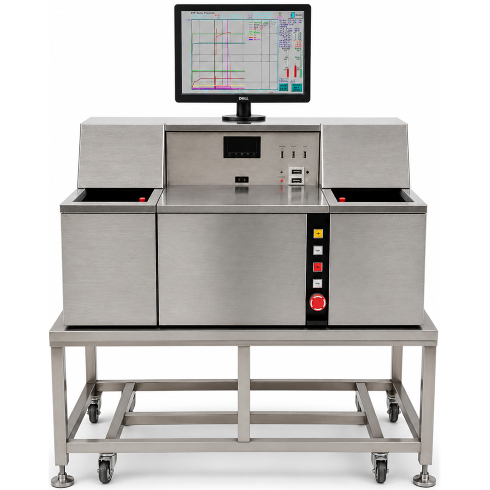
Automatic Single-Wafer Plasma Etch & RIE System
Production-Proven Plasma Etch & RIE Platform for 3“~6” High-Value Wafer Processing
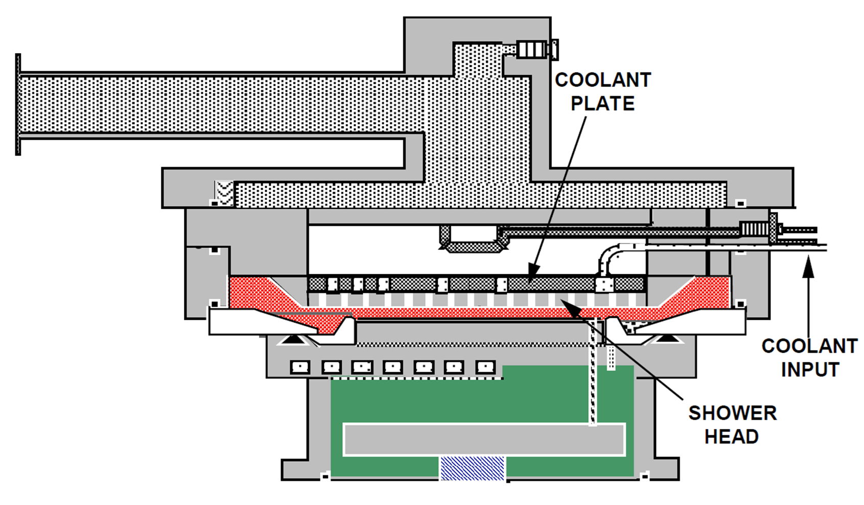
Production-Proven Reactor
Fixed-gap parallel-plate plasma etch reactor architecture supports repeatable dry etch processing for selected poly, nitride, oxide, dielectric, and descum applications.
Customer Gets:
Mature reactor architecture and lower adoption risk than a new unproven platform.
Modernized Hardware
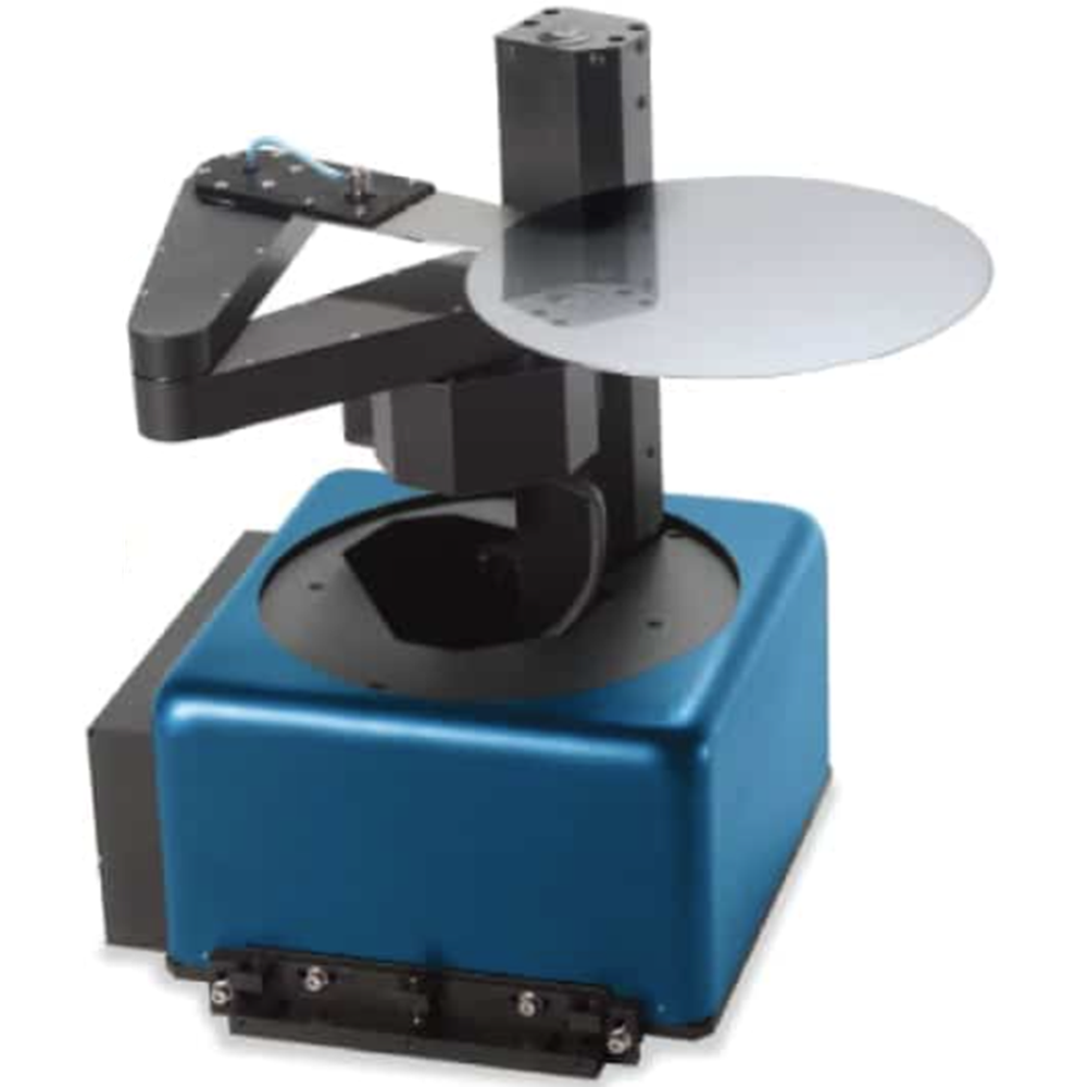
Integrated 3-axis robot, fixed cassette station, wafer aligner / cooling station, modern RF system, and updated control electronics.
Customer Gets:
Improved wafer handling reliability, easier maintenance, and reduced obsolete hardware risk.
Process-Engineer Software
Recipe control, process curve display, WTM wafer transfer, diagnostics, software calibration, subsystem testing, and optional GEM/SECS II.
Customer Gets:
Easier process setup, faster troubleshooting, and stronger fab engineering support.
The AW-901eR and AW-903eR are designed for compound semiconductor fabs, photonics device manufacturers, MEMS labs, national labs, and advanced university nano fabs where 3”–6” wafer plasma etch capability, process repeatability, wafer handling reliability, and long-term equipment support are critical.

 The AW-901eR and AW-903eR are based on a production-proven single-wafer plasma etch and RIE platform architecture widely used for 3”–6” semiconductor wafer processing.
During the growth of the semiconductor industry, mature silicon wafer manufacturing helped establish many proven process equipment platforms. Today, many compound semiconductor, photonics, MEMS, specialty device, and university nano fab applications continue to use 3”–6” wafer sizes where proven platforms remain practical and cost effective.
AW-901eR and AW-903eR support this market by preserving a mature reactor process concept while Allwin21 modernizes the equipment with robotic wafer handling, updated electronics, industrial PC control, AW-901 software, RF system options, diagnostics, calibration functions, and long-term service support.
1. Production-Proven Plasma Etch Platform
The AW-901eR / AW-903eR platform is designed for customers who need mature single-wafer plasma etch and RIE capability for 3”–6” wafer processing.
The platform is not a new experimental chamber concept. The two model configurations use different reactor gaps and pressure control ranges to support different etch material families.
Customer Gets:
- Production-proven plasma etch / RIE platform
- Clear model selection by etch material
- 3”–6” wafer process capability
- Lower adoption risk for specialty fabs and research labs
2. Modernized Allwin21 Hardware
Allwin21 modernizes the platform with integrated 3-axis robotic wafer handling, fixed cassette station, wafer aligner / cooling station function, modern RF generator options, updated electronics, and serviceable subsystem architecture.
The modernized hardware helps reduce obsolete hardware dependency while improving maintenance and long-term supportability.
Customer Gets:
- Integrated robotic wafer transfer
- Fixed cassette station with sensors
- Modernized subsystem control
- Reduced obsolete hardware risk
3. Process-Engineer Software
AW-901 control software was designed around real semiconductor process and equipment engineering requirements, not just machine operation.
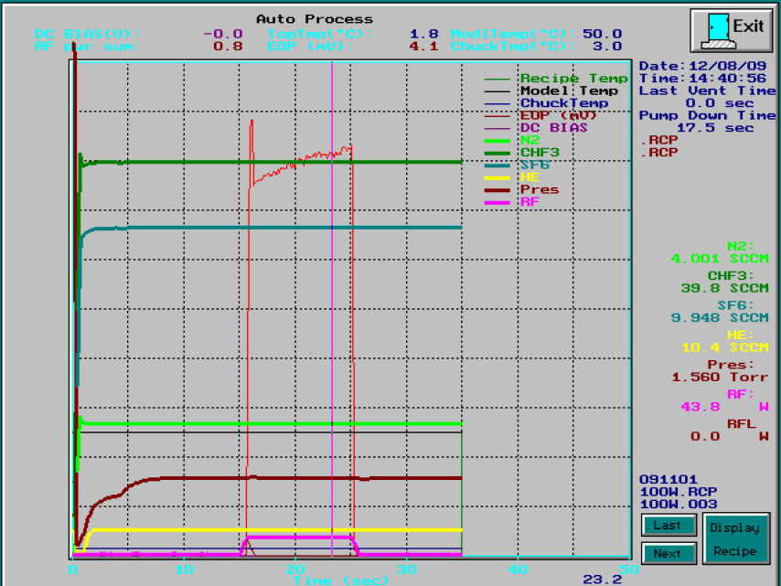
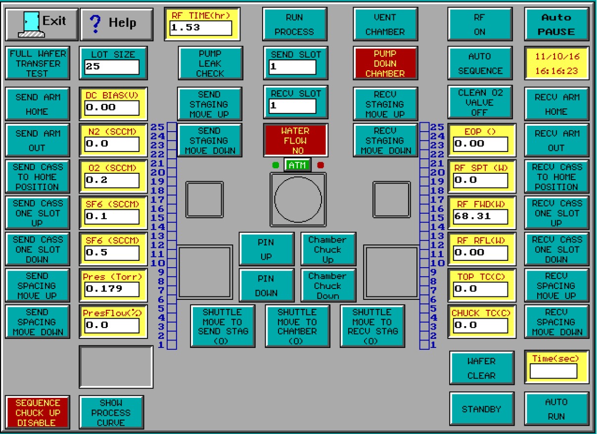
The software supports recipe editing, recipe validation, process curve display, WTM wafer transfer, subsystem diagnostics, calibration functions, board test functions, alarm management, data logging, and optional GEM/SECS II communication.
Customer Gets:
- Easier process setup
- Real-time process monitoring
- Software-based calibration support
- Faster troubleshooting capability
4. Compound Semiconductor Application Experience
The AW-901eR and AW-903eR support compound semiconductor, photonics, RF, MEMS, specialty device, and university nano fab applications where 3”–6” wafer plasma etch capability remains important.
Many of these applications continue to use mature wafer sizes and proven equipment platforms instead of high-volume 300 mm silicon fab equipment. Allwin21 supports these customers with modernized hardware, AW software, spare parts, service, and engineering support.
Customer Gets:
- Experience with 3”–6” specialty wafer applications
- Support for compound semiconductor and photonics fabs
- Model selection based on actual etch material
- Process support based on real customer applications
All trademarks belong to their respective owners.
The AW-901eR and AW-903eR share the same AW-90XeR platform, robotic wafer handling, AW-901 software, RF system options, and available options. The main difference is the reactor hardware and process window. Electrode gap, pressure control range, gas distribution design, wafer ring material, and cooling configuration make each model suitable for different etch materials.
| Item | AW-901eR | AW-903eR |
|---|---|---|
| Main Etch Materials | Polysilicon, silicon nitride, silicide, polyimide, BCB, backside etch, descum | Silicon dioxide, oxide contact, via, pad etch, passivation, dielectric etch, resist / SOG planarization, descum |
| Reactor Gap | 38 mm electrode gap | 6 mm electrode gap |
| Process Character | Poly / nitride style applications | Oxide / dielectric / contact / via style applications |
| Pressure Range | 0–1000 mTorr | 0–5000 mTorr |
| UPC Pressure Control | 225 sccm UPC | 2000 sccm UPC |
| Upper Electrode | Standard upper electrode | Advanced showerhead upper electrode |
| Lower Electrode | Standard lower electrode | Anodized lower electrode |
| Wafer Ring | Aluminum wafer ring | Ceramic wafer ring |
| Cooling Configuration | Single water recirculator configuration | Dual water recirculator configuration |
| Standard Gas Configuration | O₂, Ar, CFCl₃, SF₆ | N₂, CHF₃, SF₆, He |
| Item | AW-901eR / AW-903eR Specification |
|---|---|
| System Type | Automatic single-wafer plasma etch / RIE system.
More detailsThe AW-901eR and AW-903eR share the same AW-90XeR platform concept, robotic wafer transfer, AW-901 software, and system architecture. Final model selection depends mainly on etch material and reactor configuration.
|
| Wafer Size | 3”, 4”, 5”, and 6” round wafers.
More detailsSubstrate capability includes common 3”–6” round wafer formats used in compound semiconductor, photonics, MEMS, RF, research, and specialty device applications.
|
| Wafer Transfer | Automatic single-wafer transfer with integrated 3-axis robot. |
| RF Power | AW-901eR: standard 600W RF generator; AW-903eR: standard 1000W RF generator; 13.56 MHz.
More detailsAW-901eR is typically supplied with a 600W RF generator. AW-903eR is typically supplied with a 1000W RF generator. A 300W RF generator is available for applications requiring very low RF power operation.
|
| RF Matching | Automatic RF Matching Network |
| Electrode Gap | AW-901eR: 38 mm; AW-903eR: 6 mm. |
| Pressure Range | AW-901eR: 0–1000 mTorr; AW-903eR: 0–5000 mTorr. |
| Gas Lines | 4 gas lines with MFCs.
More detailsAW-901eR standard MFC configuration: O₂ 50 sccm, Ar 60 sccm, CFCl₃ 25 sccm, SF₆ 100 sccm. AW-903eR standard MFC configuration: N₂ 15 sccm, CHF₃ 50 sccm, SF₆ 15 sccm, He 200 sccm.
|
| Base Pressure | 20–30 mTorr.
More detailsActual base pressure depends on chamber condition, vacuum pump condition, gas configuration, and system maintenance status.
|
| Software | Allwin21 AW-901 control software. |
| Item | AW-901eR / AW-903eR Standard Configuration |
|---|---|
| Main Chassis | AW-90XeR main frame with integrated industrial PC, control electronics, EMO, interlocks, breakers, relays, AC/DC power distribution, and system wiring. |
| Reactor Chamber | Single-wafer parallel-plate plasma etch reactor. AW-901eR uses 38 mm electrode gap configuration. AW-903eR uses 6 mm electrode gap configuration. |
| Wafer Handling | Integrated 3-axis robotic wafer transfer, fixed cassette station, wafer aligner / cooling station function, cassette sensors, and wafer transfer architecture. |
| RF System | 300W, 600W, or 1000W air-cooled RF generator, 13.56 MHz, with RF matching network. |
| Gas System | 4 process gas lines with MFCs. Standard gas configuration depends on AW-901eR or AW-903eR model selection.AW-901eR-O₂, Ar, CFCl₃, SF₆, AW-903eR-N₂, CHF₃, SF₆, He |
| Pressure Control | MKS Baratron pressure measurement and UPC pressure control architecture. |
| Software | Allwin21 AW-901 control software with recipe control, real-time process monitoring, WTM wafer transfer, diagnostics, calibration, data logging, alarms, password control, maintenance support, and optional GEM/SECS II. |
| Option | Description |
|---|---|
| RF Generator Selection | AW-901eR: typically 600W ; AW-903eR: typically 1000W; 13.56 MHz.
More detailsAW-901eR: typically 600W air-cooled RF generator; AW-903eR: typically 1000W air-cooled RF generator; 13.56 MHz.300W RF generator configurations is available based on process requirements. Some low-power processes may use a 300W RF generator when the qualified process runs at low RF power such as around 50W.
|
| Optical Endpoint | Optional EOP module for endpoint monitoring and process control support. |
| GEM/SECS Interface | Optional GEM/SECS factory communication interface.
More detailsSupports communication with factory automation systems and fab host / MES integration when required.
|
| Vacuum Pump | Mechanical pump or dry pump package can be reviewed.
More detailsAllwin21 recommends customers select and purchase vacuum pumps based on their existing fab or laboratory pump standards whenever possible. Allwin21 can recommend or supply a suitable pump package when required by the project.
|
| Chiller / Recirculator Package | Temperature control package available based on AW-901eR or AW-903eR configuration. Allwin21 recommends customers select and purchase chiller based on their existing fab or laboratory chiller standards whenever possible. Allwin21 can recommend or supply a suitablechiller package when required by the project. |
| TTW Through-The-Wall Configuration | Optional through-the-wall layout for cleanroom / chase installation. |
| Alternative Gas Configuration | Alternative gas or MFC configuration can be reviewed when required by customer process. Most applications use the standard model gas configuration. |
| Spare Parts / Service | Optional spare parts kit, installation, training, process support, and engineering service. |
| Electrical | 200–240 VAC selectable, 50/60 Hz, 3-wire single phase, 30A.
More detailsMain system power. Vacuum pump power is separate and depends on pump package.
|
| Vacuum Pump Power | 208–230 / 460 VAC, 60 Hz or 200–220 / 380 VAC, 50 Hz, 3-phase, 15A.
More detailsVacuum pump electrical requirement depends on final pump package and customer facility standard.
|
| CDA / Pneumatics | 85 ±5 psig, filtered and dry.
More detailsCDA is used for system pneumatics and wafer handling related pneumatic functions.
|
| N₂ Vent / Purge / Ballast | 15 ±5 psig, filtered and dry.
More detailsN₂ is used for vent / purge / ballast functions depending on final system configuration.
|
| Process Gases | AW-901eR: O₂, Ar, CFCl₃, SF₆. AW-903eR: N₂, CHF₃, SF₆, He.
More detailsGas source regulators are required. Final gas type, purity, MFC range, and inlet pressure should be confirmed with final process configuration.
|
| Cooling Water | Distilled water in recirculating temperature control system.
More detailsTypical outlet pressure is 40 psig, 45 psig maximum. Flow rate at 40 psig is 0.4 ±0.05 GPM per loop. AW-903eR typically uses dual water recirculator configuration.
|
| Vacuum Pumping | 21 CFM minimum pumping speed at rear of system; 1.5″ ID vacuum line; NW40 interface.
More detailsVacuum pump package and vacuum line configuration should be reviewed before installation.
|
| Cabinet Exhaust | 100 CFM minimum, 4.0″ OD connection.
More detailsCabinet exhaust should be connected to facility exhaust. Vacuum pump exhaust should also be connected to proper facility exhaust or abatement according to customer safety requirements.
|
| Configuration | Equipment Dimensions | Net Weight | Shipping Dimensions | Shipping Weight |
|---|---|---|---|---|
| Desktop / Stand-Alone | 25″ H × 43″ W × 43″ D | 500 lb | 43″ H × 52″ W × 55″ D | 650 lb |
| TTW Through-The-Wall | 60″ H × 46″ W × 47″ D | 600 lb | 72″ H × 54″ W × 54″ D | 800 lb |
AW-901eR / AW-903eR automatic single-wafer plasma etch and RIE system with integrated robotic wafer handling and modernized Allwin21 control architecture.
Please provide as much information as possible in the Etcher / RIE Survey PDF and email the completed survey to sales@allwin21.com and/or allwin21corp@gmail.com.
The more complete and accurate your responses are, the better we can recommend the most suitable Etcher / RIE model or configuration for your specific needs, based on our plasma etch technology heritage and field application experience.
Completing the survey thoroughly helps ensure optimal system performance while avoiding unnecessary options that do not contribute to your application.
- Product photos and descriptions are for general reference only.
- Final configuration, specifications, options, and facility requirements shall be confirmed by official Allwin21 quotation and technical documentation.
- Process rate, etch profile, selectivity, residue-removal performance, and uniformity are application dependent.
- Facility requirements depend on final configuration and customer process requirements.
- OEM trademarks belong to their respective owners.