
Archive | Metal Film Metrology
AWgage-150 / AWgage-200 Non-Contact Conductive Thin Film Sheet Resistance Measurement System
ALLWIN21 CONDUCTIVE THIN FILM METROLOGY PLATFORM
Non-Contact Sheet Resistance Measurement for Conductive Thin Films
Compact Benchtop Metrology System for Sheet Resistance, Film Thickness Calculation, Wafer Mapping, and Process Monitoring
Proven Metrology Platform
Designed for routine conductive thin film sheet resistance measurement in fabs, universities, R&D labs, and compound semiconductor process environments.
Customer Gets:
Practical metrology capability, lower adoption risk, and fast process feedback for conductive thin film applications.
Modernized Hardware
Allwin21 updates the platform with touchscreen operation, industrial PC control, encoder-driven wafer positioning, modern electronics, and compact benchtop architecture.
Customer Gets:
Small footprint, easier operation, better serviceability, and reduced obsolete hardware risk.
AWgage Software
AWgage software supports recipe operation, calibration, wafer mapping, graphical display, data storage, diagnostics, and process-oriented metrology workflow.
Customer Gets:
Easier measurement setup, better data visibility, and stronger process monitoring support.
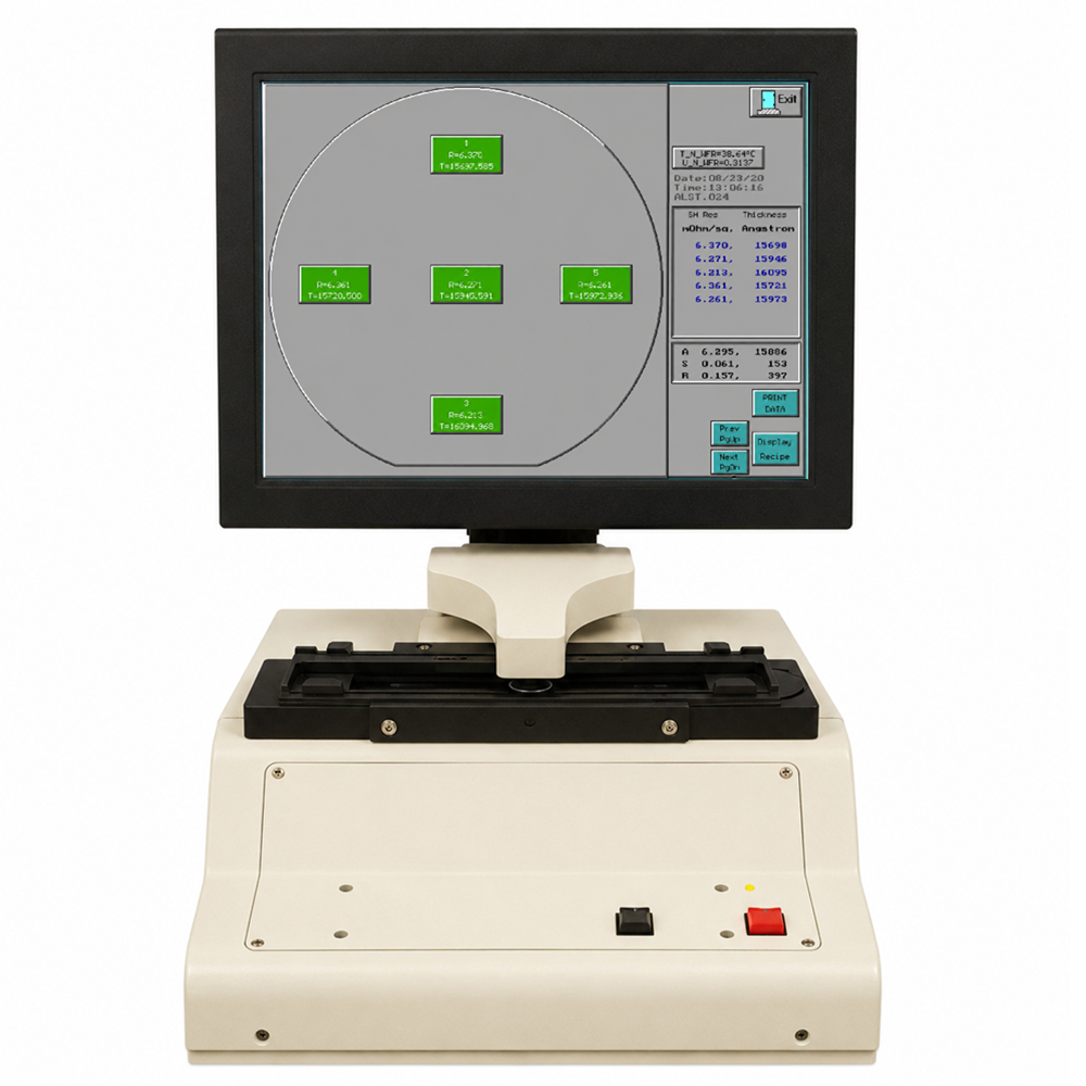
The AWgage-150 and AWgage-200 are compact non-contact conductive thin film metrology systems for measuring sheet resistance in ohms per square or milliohms per square. When material resistivity is known, film thickness can also be calculated from the sheet resistance result.
Non-Contact Conductive Thin Film Metrology Heritage
The AWgage-150 and AWgage-200 are based on a proven non-contact conductive thin film measurement architecture used for semiconductor sheet resistance monitoring, thin film process control, and wafer-level conductive film characterization.
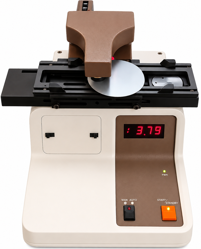
The non-contact eddy current measurement principle provides a practical method for measuring conductive thin films without physically touching the wafer surface. This helps avoid probe tip wear, probe pressure variation, and possible measurement variation caused by repeated mechanical contact.
The AWgage platform measures sheet resistance and can calculate conductive film thickness when the material resistivity is known. This makes it useful not only as a metrology instrument, but also as a process-monitoring tool for implant activation, ohmic contact alloy, silicide formation, metal deposition, RTP, RTA, diffusion, and other conductive thin film processes.
Allwin21 modernizes the platform with industrial PC control, touch-screen operation, encoder-driven wafer positioning, AWgage software, graphical wafer mapping, recipe management, calibration tools, diagnostics, data traceability, and optional factory automation communication capability.
Why Customers Choose the AWgage-150 / AWgage-200
Production-Proven Thin Film Metrology Platform
The AWgage platform is designed for conductive thin film sheet resistance measurement and process monitoring in semiconductor fabs, universities, research institutes, and thin-film laboratories.
Customer Gets: practical metrology capability, compact benchtop operation, and fast process feedback.
Modernized Allwin21 Hardware
Allwin21 modernizes the platform with touchscreen operation, industrial PC control, encoder-driven wafer positioning, updated electronics, and compact benchtop architecture.
Customer Gets: easier operation, better serviceability, and reduced obsolete hardware risk.
Process-Oriented AWgage Software
AWgage software supports recipe operation, calibration, wafer mapping, graphical display, data storage, diagnostics, and process-oriented metrology workflow.
Customer Gets: easier measurement setup, better data visibility, and stronger process monitoring support.
Non-Contact Eddy Current Measurement Technology
The AWgage-150 and AWgage-200 measure conductive thin film sheet resistance without physically touching the wafer surface.
This helps avoid probe tip wear, probe pressure variation, and contact-related measurement variation during routine process monitoring.
Customer Gets: no probe wear, no probe pressure adjustment, no physical wafer contact, and improved long-term repeatability.
Quick Specifications
| Item | Description | ||||
|---|---|---|---|---|---|
| Model Difference |
|
||||
| Measurement Technology | Non-contact eddy current sheet resistance measurement. | ||||
| Measurement Parameters | Sheet resistance measurement; conductive film thickness calculation when material resistivity is known. | ||||
| Sheet Resistance Units | Ω/sq or mΩ/sq. | ||||
| Measurement Range | 1 mΩ/sq to 19,990 Ω/sq. | ||||
| Test Points | Single center point, 5-point, or 9-point measurement. | ||||
| Wafer Stage | Encoder step motor driven programmable wafer movement. | ||||
| User Interface | Touchscreen GUI with industrial PC control. | ||||
| Software | AWgage software for recipe operation, calibration, mapping, diagnostics, and data storage. | ||||
| Factory Communication | GEM/SECS can be reviewed when required. | ||||
| Electrical | 110/220 VAC, single phase, 50/60 Hz, 2 A. | ||||
| Dimensions | Approx. 11″ W × 18″ D × 22″ H. | ||||
| Weight | Approx. 44 lbs. |
Typical Applications
Sheet Resistance MeasurementConductive Thin Film MetrologyFilm Thickness CalculationWafer MappingThin Film Process MonitoringIon Implant MonitoringOhmic Contact AlloySilicide Process MonitoringMetal Deposition MonitoringRTP / RTA Process MonitoringCompound Semiconductor MetrologyUniversity & R&D Labs
The AWgage platform is commonly used for conductive thin film sheet resistance measurement and process monitoring after RTP, RTA, implant activation, alloy, silicide, diffusion, and metal deposition processes.
Facility Requirements
| Item | Requirement |
|---|---|
| Electrical | 110/220 VAC, single phase, 50/60 Hz, 2 A. |
| Installation Surface | Place on a hard, stable surface. Do not operate the system on soft padded surfaces. |
| Environment Temperature | Stable room temperature is recommended. Around 23°C is preferred for best measurement consistency. |
| Environment Cleanliness | Avoid environments with high abrasive particle concentration, such as glass powder, silicon powder, or similar dust sources. |
| Customer Responsibility | Customer is responsible for suitable facility power, stable room environment, proper bench support, and clean operating conditions. |
The system is sensitive to room temperature stability. For best repeatability, the measurement environment should be controlled and stable.
Product Video
AWgage-150 / AWgage-200 Non-Contact Conductive Thin Film Sheet Resistance Measurement System
Important Notes
- Product photos and descriptions are for general reference only.
- Final configuration, specifications, options, and facility requirements shall be confirmed by official Allwin21 quotation and technical documentation.
- Measurement performance and repeatability are application dependent.
- Facility requirements depend on final configuration and customer application requirements.
- OEM trademarks belong to their respective owners.
Additional Metrology Keywords References
Thin Film Metrology, Conductive Thin Film Metrology, Sheet Resistance Measurement, Sheet Resistance Measurement System, Non-Contact Sheet Resistance Measurement, Non-Contact Eddy Current Measurement, Conductive Film Thickness Measurement, Film Thickness Measurement, Thin Film Thickness Measurement, Semiconductor Metrology Equipment, Semiconductor Metrology System, Wafer Metrology, Wafer Mapping, Wafer Sheet Resistance Measurement, Sheet Resistance Mapping, Metal Film Measurement, Conductive Film Characterization, Thin Film Process Monitoring, Thin Film Process Control, Semiconductor Process Monitoring, Ion Implant Monitoring, Ohmic Contact Monitoring, RTP Process Monitoring, RTA Process Monitoring, Silicide Process Monitoring, Metal Deposition Monitoring, Compound Semiconductor Metrology, GaAs Metrology, InP Metrology, GaN Metrology, SiC Metrology, Semiconductor Measurement Instrument, Conductive Film Analysis, Thin Film Characterization, Eddy Current Metrology, Wafer Thickness Calculation, Film Resistivity Measurement, KLA-Tencor, Tencor Mgage 200, Tencro Mgage 300, Tencor Sonogage 200, Tencor Sonogage 300, Mgage 200, Mgage 300, Sonogage 200, Sonogage 300, Sheet Resistance Meter, Sheet Resistance Tester