
Archive | Sputter Deposition Equipment
Home / Products / AccuSputter AW4450 RF / DC / Pulsed DC Magnetron Sputter Deposition System
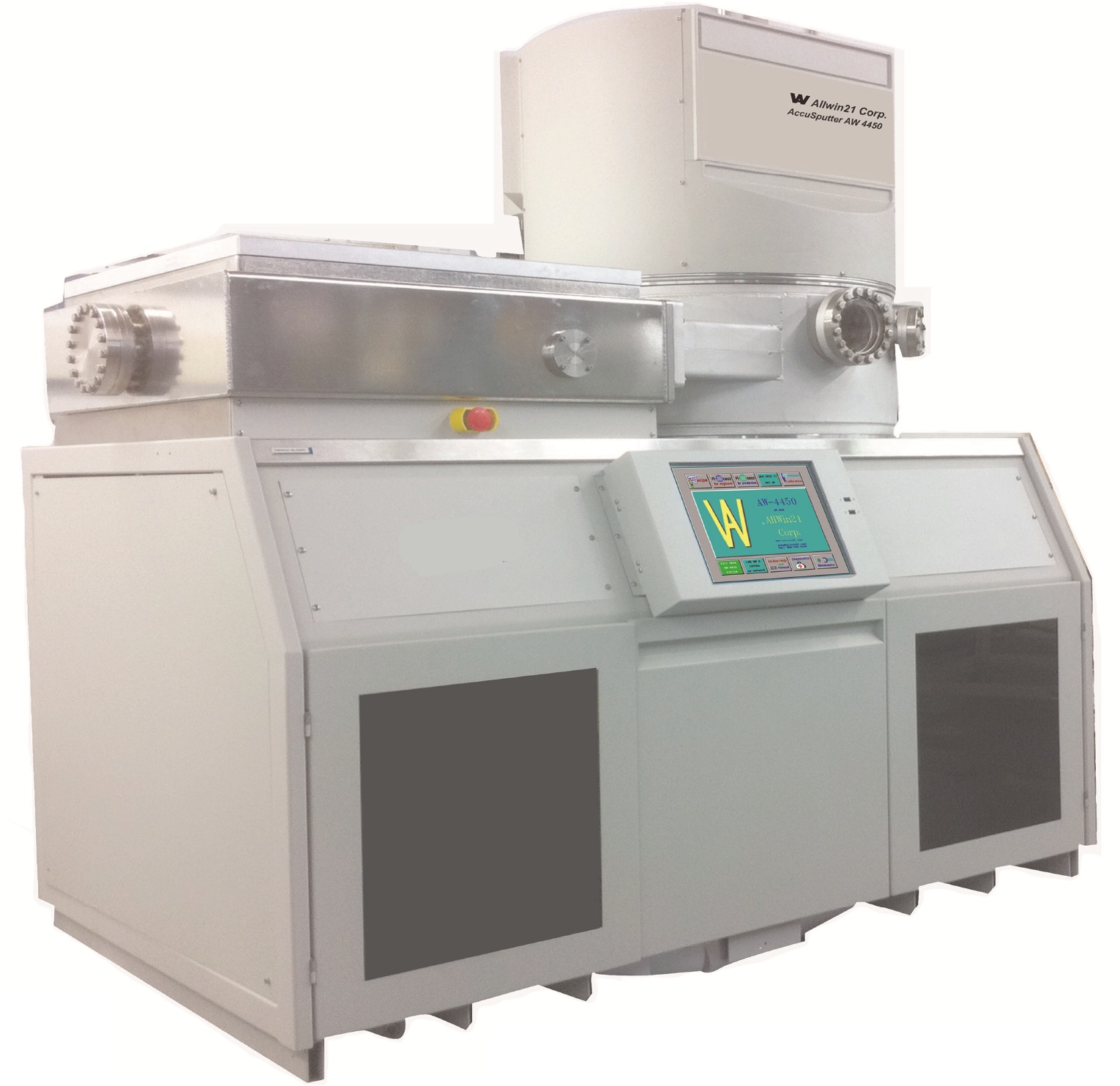
AccuSputter AW4450 RF / DC / Pulsed DC Magnetron Sputter Deposition System

Many semiconductor and compound semiconductor fabs are still running proven sputter deposition tools originally installed many years ago. These tools often remain in production because the film process works, the recipes are qualified, and the engineering team already understands the chamber behavior.
Semiconductor front-end process equipment is expensive, and the cost of making the wrong decision can be very high. A wrong equipment choice may affect qualification, production plans, engineering resources, and even the entire project direction.
AccuSputter AW 4450 Sputter: Manual, with Load Lock,RF/DC; Diode/Magnetron, Wafer Size: Small~8 inch. New Condition. ~3xDelta Shape OR ~4xCircle Shape
Perkin-ELmer 4400 Sputter: Manual, with Load Lock,RF/DC; Diode/Magnetron, Wafer Size: Small~6 inch. Refurbished and Upgraded with Allwin21 New PC controller ~4xCircle Shape
Perkin-Elmer 4410 Sputter: Manual, with Load Lock,RF/DC; Diode/Magnetron, Wafer Size: Small~8 inch. Refurbished and Upgraded with Allwin21 PC controller. ~3xDelta Shape OR ~4xCircle Shape
Perkin-Elmer 4450 Sputter: Manual, with Load Lock,RF/DC; Diode/Magnetron, Wafer Size: Small~8 inch. Refurbished and Upgraded with Allwin21 PC controller. ~3xDelta Shape OR ~4xCircle Shape
AccuSputter AW4450 RF / DC / Pulsed DC Magnetron Sputter Deposition System
ALLWIN21 SPUTTERING DEPOSITION PLATFORM
Semi-Auto Sputter Deposition Equipment
Production-Proven Magnetron Sputtering Platform for Semiconductor, Optoelectronic and Advanced Thin Film Applications
Production-Proven Sputtering Platform
Built on a production-proven magnetron sputtering architecture for semiconductor, photonics, compound semiconductor, MEMS, sensor, optical coating, and advanced thin-film deposition applications.
Customer Gets:
Lower technology risk, proven chamber performance, established process capability, and faster transition into real deposition applications.
Modernized Hardware
Allwin21 improvements include RF / DC / Pulsed DC power integration, embedded industrial computer architecture, updated motion control, modern vacuum and process control hardware, improved safety systems, simplified maintenance access, and long-term spare parts support.
Customer Gets:
Better reliability, reduced obsolete component risk, easier maintenance, improved serviceability, and longer equipment service life.
Process-Oriented Software
AW4450 software supports recipe management, deposition process monitoring, vacuum diagnostics, cathode control, substrate motion control, alarm history, maintenance functions, calibration tools, I/O monitoring, and engineering-level system visibility.
Customer Gets:
Easier process development, faster troubleshooting, better engineering visibility, and stronger long-term fab support.
The AccuSputter AW4450 is a configurable RF, DC, and Pulsed DC magnetron sputter deposition platform for semiconductor fabs, compound semiconductor manufacturers, photonics facilities, research institutes, and university laboratories requiring production-proven thin film deposition capability, flexible chamber configuration, engineer-driven software, and long-term Allwin21 support.

CE Marked Equipment • SEMI Member Since 2007 •Thin Film Deposition Solutions
Magnetron Sputtering Technology Heritage

The AW4450 is based on production-proven 4400 / 4410 / 4450 sputter deposition system technology for development and production thin film applications.
The original platform was designed for load lock operation, high vacuum sputter deposition, substrate rotation, Delta cathode and 8-inch circular cathode configurations, RF and DC sputtering, gas control, and flexible process development or production use.
Allwin21 modernizes this proven sputter platform with embedded computer control, AW4450 software, updated electronics, modern motion control, vacuum and process diagnostics, recipe control, calibration functions, data storage, and long-term service support.
This approach helps customers keep proven chamber behavior and sputter process continuity while reducing obsolete controller and electronics risk.
Why Choose the AccuSputter AW4450
1. Production-Proven Sputter Deposition Hardware
The AccuSputter AW4450 is built on a production-proven sputter deposition platform designed for thin film development and production applications. The system combines a semi-auto load lock, high-vacuum process chamber, rotating substrate table, RF and DC sputtering capability, Delta cathodes, circular cathodes, and flexible process configurations.
The platform supports RF magnetron sputtering, DC magnetron sputtering, Pulsed DC sputtering, RF bias sputtering, RF diode sputtering, reactive sputtering, and co-sputtering applications for a broad range of thin film materials.
Customer Gets:
- Production-proven sputter deposition hardware
- Flexible process chamber architecture
- RF, DC, and Pulsed DC sputtering capability
- Lower technology and qualification risk
2. Modernized Allwin21 Hardware
Allwin21 modernizes the proven platform with embedded industrial computer architecture, updated electronics, modern motion control, vacuum diagnostics, gas control hardware, safety systems, and long-term spare parts support.
The modernization strategy preserves the proven sputter chamber and process philosophy while reducing risks associated with obsolete controllers, computers, electronics, and unsupported hardware.
Customer Gets:
- Reduced obsolete hardware risk
- Improved reliability and serviceability
- Easier maintenance and troubleshooting
- Long-term hardware support
3. Process-Oriented AW Software
AW4450 software is designed for process engineers and equipment engineers. The software supports recipe editing, automatic operation, diagnostics, calibration functions, vacuum monitoring, gas control, motion control, alarm history, subsystem testing, and process data management.
The software architecture helps engineers monitor system operation, troubleshoot equipment issues, maintain process consistency, and support long-term production or R&D activities.
Customer Gets:
- Easier recipe setup and modification
- Real-time system monitoring
- Faster troubleshooting capability
- Improved engineering visibility and support
4. Trusted by Semiconductor, Compound Semiconductor, Photonics, MEMS, and Research Customers
Production-proven sputter deposition platforms continue to be widely used for semiconductor metallization, compound semiconductor processing, photonics devices, MEMS fabrication, sensor development, optical coatings, university nano fabs, and national laboratory research programs.
The AW4450 platform supports thin film deposition applications for GaAs, InP, GaN, silicon, glass, ceramic, optical, and other advanced substrate technologies requiring repeatable sputter deposition capability and long-term support.
Customer Gets:
- Production-proven platform acceptance
- Lower adoption and qualification risk
- Broad application flexibility
- Long-term process and equipment support
Real Fab & Equipment Insights
1. What Are Sputter Deposition, RF, DC, Pulsed DC, Cathode, Target, Reactive Sputter, Co-Sputter and Bias?
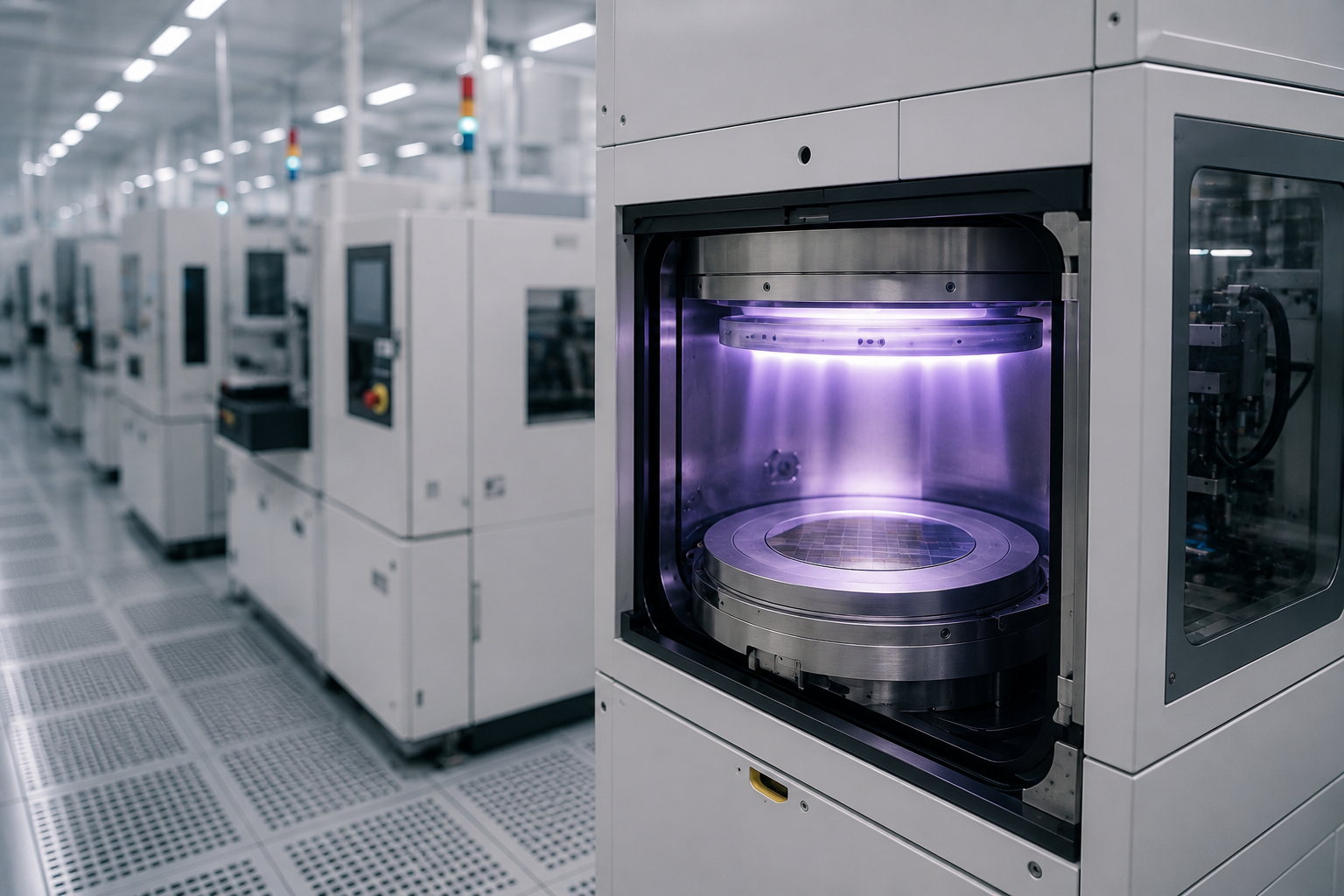
Sputter deposition is a PVD thin film deposition method. In sputtering, ions from a plasma strike a solid target. Atoms are knocked out from the target surface and then deposit on the substrate to form a thin film.
A sputter target is the source material to be deposited. A cathode is the sputter source assembly that holds the target, provides electrical power, cooling, and magnetic field configuration when magnetron sputtering is used. In magnetron sputtering, magnets help confine electrons near the target surface, improving plasma density and deposition rate.
DC sputtering is normally used for conductive targets such as Al, Ti, Cr, Au, Pt, W, Ni, TiW and similar metal films. RF sputtering, commonly at 13.56 MHz, is used when the target is insulating or difficult to run with DC power. Pulsed DC sputtering is often used for reactive sputtering and compound film deposition from conductive targets, helping reduce arcing when insulating material builds up on the target surface.
Reactive sputtering means adding a reactive gas, such as oxygen or nitrogen, during sputtering so the sputtered material reacts and forms a compound film such as oxide or nitride. Co-sputtering means sputtering from two or more targets to form an alloy, compound, or multilayer film. RF bias or DC bias applies power to the substrate side to influence ion energy, adhesion, film density, stress, step coverage, or pre-clean / sputter-etch behavior.
Sputtering is often selected for compound semiconductor, photonics, MEMS, sensor, optical coating, and semiconductor metal applications because it can deposit metals, alloys, oxides, nitrides, transparent conductive films, and multilayer films. Compared with evaporation, sputtering does not require melting the source material and is often better for alloys, refractory metals, compound films, adhesion layers, and process control. Evaporation can be useful for many metals and lift-off processes, but sputtering is often preferred when film density, adhesion, alloy composition, reactive films, and repeatable process control are important.
2. Why Production Fabs Continue Using Proven Sputter Deposition Tools
There are many sputter deposition equipment suppliers in the semiconductor industry. Many tools can deposit a metal film in a short test. Production fabs usually look deeper than that.
For a sputter deposition tool, the chamber geometry, cathode type, target size, substrate rotation, pallet design, load lock, pumping system, pressure control, gas control, RF/DC power behavior, shutter timing, and process sequence can all affect film rate, thickness uniformity, stress, resistivity, adhesion, particles, and step coverage.
This is why production fabs often continue using qualified sputter platforms for many years. Once Al, Ti, TiW, Au, Cr, Pt, W, Ni, ITO, oxide, nitride, or multilayer films are qualified, changing to a different chamber design may require process requalification, film characterization, reliability checks, and engineering time.
The original 4400/2400 brochure described these tools as sputter deposition systems for development and production, with load lock operation, high vacuum pumping, gas controllers, RF/DC power options, Delta cathode and circular cathode configurations, substrate rotation, and flexible process capability. Those are still the reasons many fabs prefer proven sputter deposition tools instead of changing chamber platforms without a strong need.
Customers evaluating sputter tools should therefore compare not only maximum power or target count. Important topics include film history, cathode configuration, target utilization, wafer loading, substrate rotation, vacuum system, pumpdown behavior, pressure control, process repeatability, spare-parts support, and the ability to keep qualified recipes running.
4. Legacy Sputter Tool Support and Process Continuity
 Many semiconductor and compound semiconductor fabs are still running proven sputter deposition tools originally installed many years ago. These tools often remain in production because the film process works, the recipes are qualified, and the engineering team already understands the chamber behavior.
At the same time, many fabs now face support problems from obsolete computers, old control electronics, motion hardware, RF/DC power interfaces, vacuum gauge controls, cryopump controls, and OEM-specific boards. One failed board or old computer can stop a qualified sputter process even when the chamber, cathodes, pumps, and process hardware are still usable.
The difficult part is that many fabs cannot simply replace a proven sputter tool with a completely different system. The film rate, uniformity, stress, resistivity, adhesion, step coverage, target behavior, and maintenance method may already be tied to production yield and long-term fab experience.
Allwin21 supports this type of fab need by rebuilding, reforming, and upgrading proven sputter platforms with embedded computer control, AW-4450 software, updated electronics, modern motion control, vacuum and process diagnostics, recipe control, calibration functions, data storage, and long-term service support while keeping the proven chamber and sputter process concept.
This approach helps fabs reduce obsolete control risk while keeping process continuity for qualified sputter deposition applications.
5. Why Semiconductor Front-End Equipment Purchasing Is Different
 Semiconductor front-end process equipment is expensive, and the cost of making the wrong decision can be very high. A wrong equipment choice may affect qualification, production plans, engineering resources, and even the entire project direction.
It is also technically complex. Sputter results depend on process chamber configuration, cathode type, target material, substrate type, wafer size, substrate rotation, RF/DC power, pressure, gas flow, vacuum condition, pump configuration, recipe, and measurement method. The same film result achieved in one fab may not be achieved in another fab without process work.
This is why experienced suppliers ask key RFQ questions early.
| RFQ Topic | Why It Matters |
|---|---|
| Budget Range | Budget helps quickly narrow the suitable equipment level and avoid wasting time on the wrong platform. In many cases, configuration can be adjusted to reduce cost without affecting the real process requirements. |
| Real Process Requirement | Target film material, wafer size, substrate type, film thickness, uniformity target, rate target, stress, resistivity, adhesion, step coverage, reactive gas need, co-sputter need, RF bias / DC bias need, and production or R&D use all affect the correct equipment recommendation. |
| Configuration and Facility Fit | Cathode type, target size, RF/DC/Pulsed DC power, gas lines, MFC range, load lock, vacuum pump, cryopump, cooling water, CDA / N₂, exhaust, electrical power, installation, training, and spare-parts support should be confirmed before final quotation. |
For AW4450 projects, the most important point is to confirm whether the customer needs a production-proven sputter deposition tool for qualified thin film processes, flexible RF/DC/Pulsed DC sputtering, reactive sputtering, co-sputtering, or a modernized replacement / upgrade path for an existing legacy sputter platform.
Quick Specifications
| Item | AW4450 Capability |
|---|---|
| Wafer / Substrate Size | Small samples to 8-inch wafers typical. The system supports semiconductor wafers, compound semiconductor wafers, optical substrates, glass, ceramic, metal, plastic and custom substrates. |
| Wafer Loading | Semi-auto load lock system with pallet transfer between load lock and process chamber. |
| Pallet and Typical Quantity per Run | 23-inch diameter annular molybdenum pallet with 7-inch center opening for table lift and rotation mechanism. Typical quantity per run: 30 × 3-inch wafers, 22 × 100 mm wafers, 10 × 125 mm wafers, 8 × 150 mm wafers, or 5 × 8-inch wafers.
More detailsThe annular Mo pallet provides 8-inch radial loading width. Actual deposition rate, film uniformity, and throughput depend on substrate quantity, substrate placement, target material, cathode configuration, sputter power, process pressure, film thickness, and recipe.
|
| Cathode Configuration | Basic system includes one RF magnetron cathode or one DC magnetron cathode. Customer can select one 8-inch circular cathode or one Delta cathode. |
| Sputter Methods | RF magnetron sputtering, DC magnetron sputtering, Pulsed DC magnetron sputtering, RF diode sputtering, RF sputter etch / clean, RF bias sputtering, reactive sputtering, and co-sputtering depending on configuration. |
| RF / DC / Pulsed DC Power | Basic system includes either 1 kW RF power or 5 kW DC power. Optional configurations include 2 kW RF generator, 10 kW DC power supply, and 5 kW Pulsed DC power supply.
More detailsRF, DC, and Pulsed DC power configuration depends on target material, cathode type, film requirement, and process application. RF matching network is required for RF sputtering, RF clean / etch, RF bias, and RF diode sputtering.
|
| Process Materials | Demonstrated materials include Al, Al+Ti/W+Ag, Al2O3, Au, C, Cr, Cr/Co, Cr/Au, Cr+Cu, Cr/Si, Cr/SiO, Cr/SiO2, InSnO, Mo, MoSi2, Mo2Si5, Mo5Si3, Ni, Ni/Cr, Ni+Ni/Cr, Ni/Fe, Ni/Fe+Cu+SiO2, Pt, SiC, SiO2, SiO2+O2, Si+N2 / Si3N4, Si+N2+B4C, Ta, TaC, Ta+Au, TaSi2, Ta+SiO2, TiO2, TiO2+Cr, Ti+Au, Ti+Au+Ni, Ti/W, Ti/W+Au, Ti/W+Au+Ta, Ti/W+Al/Si, Ti/W+Ni/Cr+Au, Ti/W+Pt, W, W+Al2O3, Zn, ZnO2, and Zr. |
| Gas Lines and Process Gases | Basic system includes one 200 SCCM Ar MFC. Optional gas configuration supports up to 3 gases with MFCs. Typical gases include Ar, O2, and N2. |
| Base Pressure | Typical high vacuum base pressure is in the 10-7 Torr range with cryopump configuration. |
| Process Pressure | Typical sputter process pressure is around several mTorr. Published Al-1%Si process example uses 8 mTorr Ar pressure. |
| Typical Deposition Rate | Published Delta cathode aluminum alloy data shows instantaneous deposition rate up to 12,000 Å/min, with specific rate over the entire substrate pallet in excess of 200 Å/kW-minute and target utilization approaching 60%. |
| Film Uniformity | Published Delta cathode data shows typical uniformity related to wafer size and loading quantity: 30 × 3-inch wafers ±7%, 22 × 100 mm wafers ±5%, 10 × 125 mm wafers ±7%, 8 × 150 mm wafers ±12%, and 5 × 8-inch wafers ±14%.
More detailsFilm uniformity depends on wafer quantity, wafer position on the Mo pallet, target material, target condition, cathode configuration, substrate rotation, process pressure, sputter power, and process recipe.
|
| Film Thickness Range | Thin films range from a few Angstroms up to several microns depending on process and material. |
| Typical Process Results | Published Al-1%Si process example: 9 kW DC power, table rotation 10 rpm, Ar pressure 8 mTorr, film thickness 1.04 µm, deposition time 5.8 minutes, step height 1.10 µm, step slope 80°, step coverage 62%, specularity 65–75%, resistivity 2.85 µΩ-cm, and grain size 2 µm.
More detailsActual deposition rate, film thickness, uniformity, resistivity, stress, adhesion, step coverage, and throughput depend on target material, cathode configuration, substrate loading, vacuum condition, power, pressure, gas flow, and recipe.
|
Typical process data and performance values are application dependent. Final process rate, uniformity, film properties, throughput, and acceptance criteria should be confirmed based on customer material, substrate size, pallet loading, target configuration, process condition, recipe, and metrology method.
Standard Configuration
| Item | AW4450 Basic System Configuration |
|---|---|
| Main Frame and System Body | AW4450 main frame with process reactor chamber, load lock, table lift / rotation mechanism, vacuum hardware, gas control hardware, power distribution, safety interlocks, and system wiring. |
| Load Lock with Elevator | Load lock chamber with elevator transfer for semi-auto wafer / pallet loading between load lock and process reactor chamber. |
| Process Reactor Chamber | Process reactor chamber with rotating table, cathode port, shutter function, substrate pallet support, vacuum interface, gas inlet, and process pressure control hardware. |
| Cathode | One RF magnetron cathode or one DC magnetron cathode. Customer can select one 8-inch circular cathode or one Delta cathode for the basic system. |
| RF or DC Power | Basic system includes either 1 kW RF power with RF matching network or 5 kW DC power supply depending on selected cathode and process requirement. |
| Vacuum System | Cryopump with compressor, high-vacuum valve, vacuum gauges, vacuum meters, roughing connection, and related vacuum control hardware. |
| Gas System | One 200 SCCM Ar MFC with gas valve and gas control interface. |
| Mo Pallet | One 23-inch annular molybdenum pallet with customer-defined pockets for wafer or substrate loading. |
| AW Controller | AW controller with embedded industrial computer, distributor board, DC power distribution, machine interface electronics, control wiring, and operator monitor. |
| AW4450 Software | AW4450 control software with recipe editing, manual operation, automatic operation, diagnostics, calibration functions, vacuum control, gas control, power control, motion control, alarm / data records, and process data storage. |
Optional Configuration
| Option | Description |
|---|---|
| Additional Cathodes | System can be configured with up to 4 × 8-inch circular cathodes or up to 3 × Delta cathodes.
More detailsCathode quantity depends on selected cathode type, power configuration, substrate heating requirement, co-sputtering requirement, and process chamber configuration.
|
| Additional Gas Lines | Up to 3 process gases with MFCs can be configured. Typical gases include Ar, O2, and N2. |
| RF Clean / RF Etch Function | Optional RF clean / RF etch function with 1000 W RF generator and RF matching network. |
| RF Bias Function | Optional RF bias function with 500 W RF generator and RF matching network.
More detailsRF bias can be used with RF magnetron sputtering, DC magnetron sputtering, or Pulsed DC magnetron sputtering depending on process configuration.
|
| Higher RF Power | Optional 2 kW RF generator with RF matching network for RF sputtering applications requiring higher RF power. |
| Higher DC Power | Optional 10 kW DC power supply for DC magnetron sputtering applications. |
| Pulsed DC Power | Optional 5 kW Pulsed DC power supply for Pulsed DC magnetron sputtering and selected reactive sputtering applications. |
| Load Lock Heating / Degas | Optional load lock heating / degas function for substrate preheating or moisture reduction before process transfer. |
| Reactor Substrate Heating | Optional reactor substrate heating function.
More detailsReactor substrate heating occupies one cathode port. If reactor heating is selected, the maximum available cathode quantity is reduced by one.
|
| RF Diode Sputtering | Optional RF diode sputtering configuration without magnetron cathode. |
| Pulsed DC Sputtering | Optional Pulsed DC sputtering configuration for selected conductive targets and reactive sputter processes. |
| Reactive Sputtering | Optional reactive sputtering configuration using process gases such as O2 or N2 for oxide, nitride, or compound film deposition. |
| Co-Sputtering | Optional co-sputtering configuration for alloy, compound, multilayer, or process-development applications using more than one cathode. |
| Load Lock Turbo Pump | Optional turbo pump configuration for load lock pumping. |
| Turbo Pump Vacuum System | Optional turbo pump system can be configured instead of cryopump and compressor for selected R&D applications. |
| Mechanical Pump or Dry Pump | Mechanical pump or dry pump configuration can be reviewed for cryopump roughing, load lock pumping, or customer facility preference. |
| Meissner Trap | Optional Meissner Trap for additional water vapor pumping capability. |
| GEM / SECS Interface | Optional GEM / SECS factory communication interface for fab host or MES communication. |
| Spare Parts / Service | Optional spare parts kit, installation, training, process support, engineering service, and long-term maintenance support. |
| Enhanced Table Lift Feedthrough Assembly | Upgraded substrate table lift up/down feedthrough assembly for easier maintenance, reduced vacuum leak risk, and improved long-term reliability. |
Typical Applications
RF Magnetron Sputtering DC Magnetron Sputtering Pulsed DC Sputtering RF Diode Sputtering Reactive Sputtering Co-Sputtering RF Bias Sputtering RF Sputter Etch Metal Thin Films Alloy Thin Films Oxide Films Nitride Films Aluminum Alloy Deposition Gate Contact Metallization Interconnect Metallization III-V Materials GaAs InP GaN Compound Semiconductor Photonics Devices Optoelectronics MEMS Sensors Optical Coatings University Nano Fabs National Labs
AW4450 is used for sputter deposition of metal, alloy, oxide, nitride, dielectric, optical, and multilayer thin films. Typical applications include semiconductor metallization, aluminum alloy deposition, adhesion / barrier layers, compound semiconductor metallization, photonics, MEMS, sensors, optical coatings, and R&D thin film development.
Facility Requirements
| Item | Facility Requirement |
|---|---|
| Facility Interface Panel | Rear-mounted electrical, cooling water, process gas, CDA, and LN2 inlet panel with integrated power distribution box, water flow switch panel, and utility manifold. |
| RF / DC Power | 208 VAC, 60 Hz, 3 Phase, 60A, 4 wires. |
| Vacuum System Power | 208 VAC, 60 Hz, 3 Phase, 60A, 5 wires. |
| Cooling Water | 1.8 GPM minimum cooling water supply required. |
| Process N2 | 60–70 PSI. |
| Process Argon | 5–10 PSI. |
| CDA | 40–60 PSI clean dry air. |
Dimensions and Weight
| Item | Information |
|---|---|
| Equipment Dimensions | 65″ W × 46″ D × 68″ H |
| AW4450 Net Weight | Approximately 2,288 lbs |
| Shipping Crate Dimensions | 59″ W × 78″ D × 83″ H |
| Shipping Weight | Approximately 2,600 lbs |
The shipping dimensions and weight listed above are typical for a standard AW4450 sputter deposition system with load lock, process chamber, vacuum system, and controller. Final shipping dimensions and weight depend on cathode quantity, RF/DC/Pulsed DC power configuration, substrate heating options, vacuum system selection, and customer-selected options.
Product Video
AccuSputter AW4450 RF, DC, and Pulsed DC Magnetron Sputter Deposition System
Important Notes
- Product photos and descriptions are for general reference only.
- Final configuration, specifications, options, and facility requirements shall be confirmed by official Allwin21 quotation and technical documentation.
- Process rate, residue-removal performance, and uniformity are application dependent.
- Facility requirements depend on final configuration and customer process requirements.
- OEM trademarks belong to their respective owners.